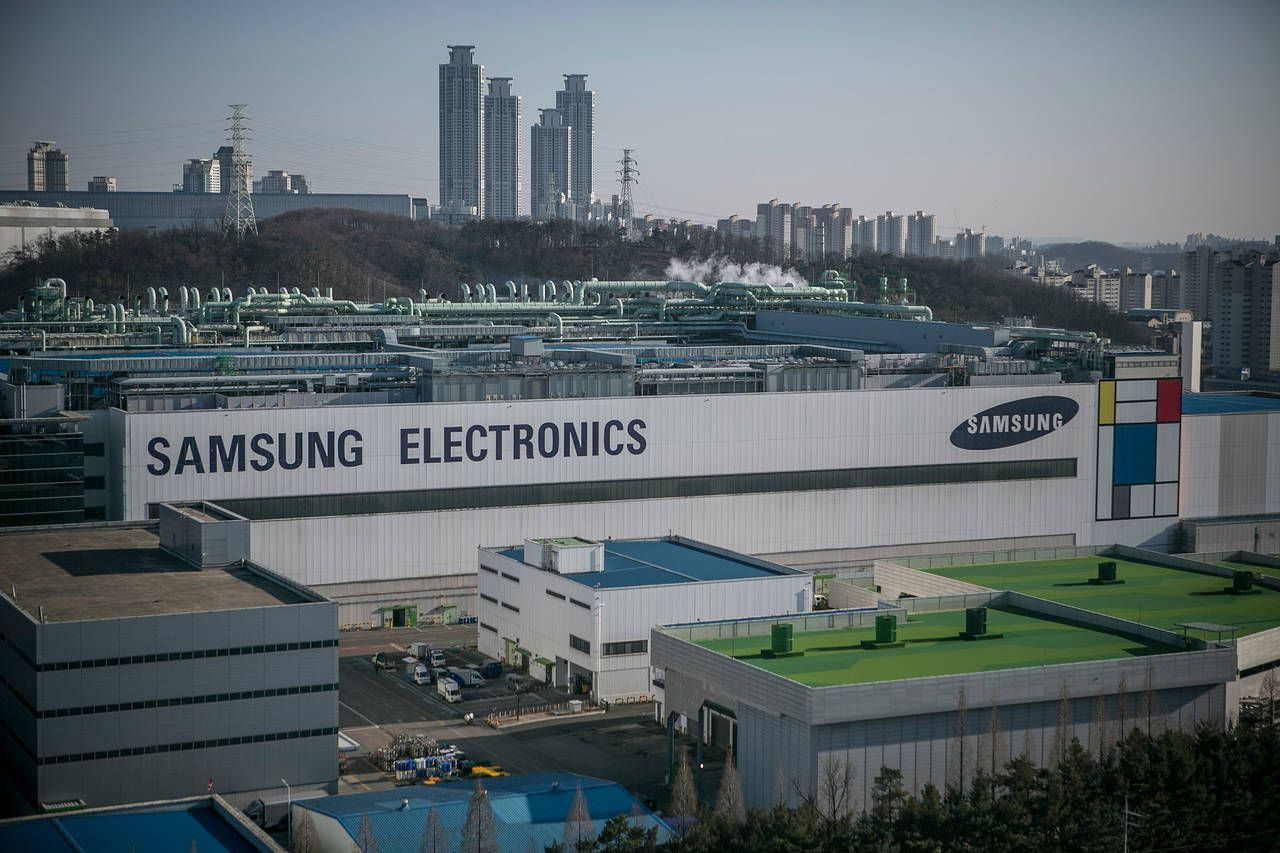
Samsung Electronics dropped some big news at Computex 2026 in Taiwan, unveiling their HBM5 tech. This fresh gear features a thermal management system called HPB, along with some serious production breakthroughs for next-gen memory chips.
The HPB technology employs a chimney-like thermal structure that cuts down thermal resistance between the chips. It channels heat away from the main die and base die through specialized heat-dissipating columns, directing it to a heat spreader at the top of the package or outside it. Samsung claims this method allows for heat dissipation without complicating the design of the HBM main dies or the stacking layout of HBM.
In HBM5, Samsung plans to utilize a 2nm base die, unlike the 4nm base die used in HBM4 and HBM4E. The company will leverage GAA nodes from Samsung Foundry to boost performance and energy efficiency. For the main HBM dies, a 1cnm interface process will be employed with partial implementation of hybrid bonding technology.
The company stated that it is ready to roll out HCB technology and has amassed GAA data over the past three to four years.
Citi analysts noted: "We expect Samsung Electronics to significantly enhance the thermal stability of HBM through the adoption of HPB technology, which is already utilized in Samsung's mobile SoC — Exynos 2600."
Analysts also noted that Samsung will use its 2nm production node to manufacture the HBM5 base die, creating synergy between its memory and contract manufacturing divisions.
#MarketCorrection #HighTechNews
In our group, we typically retain those subscribers who, in search of fresh and relevant news, don't want to sift through dozens of different sites and news outlets and can afford to read all the most interesting updates in one news feed!!! 😉
Enjoy your viewing!!! 😊
Meanwhile, we'll keep hunting for fresh and interesting news. 🤫